Plenary Speakers
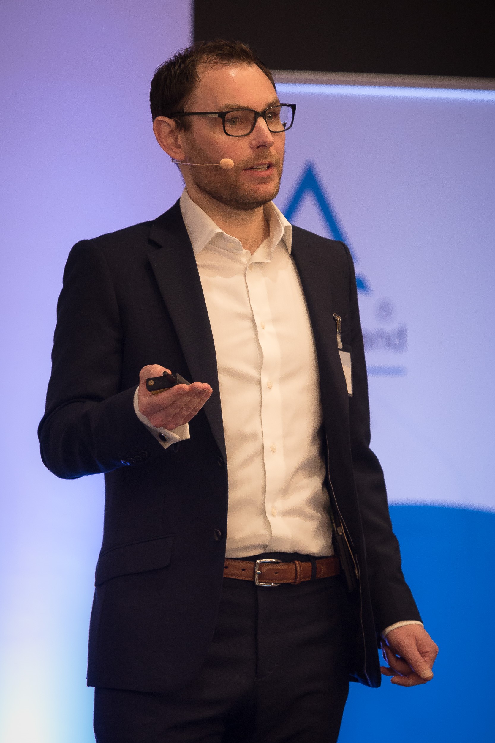 James Blakesley
National Physical Laboratory
United Kingdom
Seeing into devices: New optical techniques for device characterisation
James is a Principal Research Scientist and Science Area Leader for Electronic and Magnetic Materials at the National Physical Laboratory, United Kingdom. He specialises in the development of measurement techniques for new and emerging devices, materials and applications, particularly in photovoltaic technologies. The aim is to apply measurement science to improve performance, quality and yield of devices and to accelerate the translation of emerging technologies from basic research to application. He is also an IEC technical committee expert and contributes to the development of performance standards for photovoltaics and emerging electronic materials. James obtained a PhD from the University of Cambridge for work on novel single-photon detectors for quantum cryptography. He worked at University College London, the University of Cambridge and Potsdam University on projects including novel x-ray detectors, charge transport in organic semiconductors and new photovoltaic materials. Since then, he joined NPL, the UK’s national metrology institute, where he has worked for 10 years.
 Dr Anne Hémeryck
LAAS-CNRS
Toulouse
France
Formation of defects in semiconductors: what contribution from atomistic modeling?
Anne Hémeryck has been a full-time researcher at the Laboratory for Analysis and Architecture of Systems at the French National Centre for Scientific Research (CNRS) since 2011. In April 2016, she created the M3 Team at LAAS-CNRS for Multilevels Modeling of Materials. She is nowadays the Head of the M3 Research Team. Since nearly 16 years, Anne Hémeryck performs intensive calculations to address materials science issues. During all her past professional experience, she always focused her research activities on modeling and simulation approaches dedicated to a variety of microelectronics topics, such as silicon oxidation (PhD in CEA-DAM, Arpajon, France), catalysis activity at the surface a gas sensor (postdoctoral fellow in LAAS-CNRS, Toulouse, France), nanoindentation simulations and hydrogen production enhanced by Al supernanoparticle (Postdoc fellow in University of Southern California in Priya Vashishta’s Team, Los Angeles, USA), preparation and coating of surface through molecular passivation and functionalization (6 months contractual work at the IRCP, Paris, France), assembly of nanoparticles thanks to DNA (in 2012 in LAAS-CNRS). Her research focuses on the nanoengineering of materials encountered in microelectronics by considering them in an atomic point of view and focus on the critical issue of the surface and interface phenomena and properties. She aims at focusing on the development and application of multi-levels computational methods, dedicated to physical and chemical problems in material science, notably on the predictive simulation concerning properties of materials directly integrated.
 Prof Dr Layla Martin-Samos Colomer
CNR-IOM Democritos
Trieste
Italy
Defect signatures in semi-conductors and insulators: understanding and modeling
Prof. Dr. Layla Martin-Samos is a researcher from the Italian National Research Council (CNR-IOM) leading a group of three postdocs and one PhD student. She is also external associated professor at the University of Nova Gorica. After a PhD in Computational Material Science in Paris (2004) devoted to the modelling of defects in amorphous SiO2 from first-principles, she moved to the INFM-S3 center in Modena (Italy) where she developed SaX (Self-energies And eXitations), a software package based on Many-Body Perturbation Theory. SaX was the first Open Source freely available software released (GPL) for the modelling of electronic excitations, including optical excitations, within the GW approximation and the Bethe-Salpeter Equation. In 2009, she moved to Trieste (Italy) where she worked as development scientist for Quantum ESPRESSO. In 2012 she became assistant Professor at the University of Nova Gorica (Slovenia) in the Materials Research Laboratory. Her research interests include software development, refactoring and optimization (enabling High Performance Computing and High Through Put) and connection between theory and experiments, including multi-scaling and methodological developments. She is actively involved in a longstanding multi-partner collaboration (CEA-DIF, CNRSLAAS and SISSA), devoted to understanding and modeling defects and irradiation effects in semiconductors and insulators. She also participates in the activities of the Electronic Structure Library initiative and she is member of the psi-k (Ab-initio calculation of complex processes in materials) working group ‘Software engineering’. She is author/co-author of more than 50 papers published in peer reviewed international journals. She is PI of WP4 ‘Multi-Scale Modeling’ of H2020 FETOPEN MAGNELIQ and project manager of several industrial research contracts.
 Prof Dr Bryce S Richards
Institute for Microstructure Technology (IMT)
Nanophotonics for Energy, Faculty of Electrical Engineering and Information Technology, Karlsruhe Institute of Technology (KIT), Eggenstein-Leopoldshafen
Germany
A load of rubbish or a big opportunity for luminescent materials?
Bryce Richards studied physics at the Victoria University of Wellington (New Zealand) before completing a Masters and PhD in electrical engineering at Univ. of New South Wales (Australia), in 1998 and 2002, respectively. He worked at both UNSW and the Australian National University. In 2006, he joined Heriot-Watt University (Edinburgh, U.K.) as a lecturer, being promoted to full professor in 2008. Since 2014 he is co-director of the Institute for Microstructure Technology (IMT) and Light Technology Institute (LTI) within the Karlsruhe Institute of Technology (Germany). His primary research areas lie in third generation photovoltaics (including perovskite solar cells), spectral conversion (up- and down-conversion), luminescent materials, light management, and solar-powered water treatment systems.
Invited Speakers
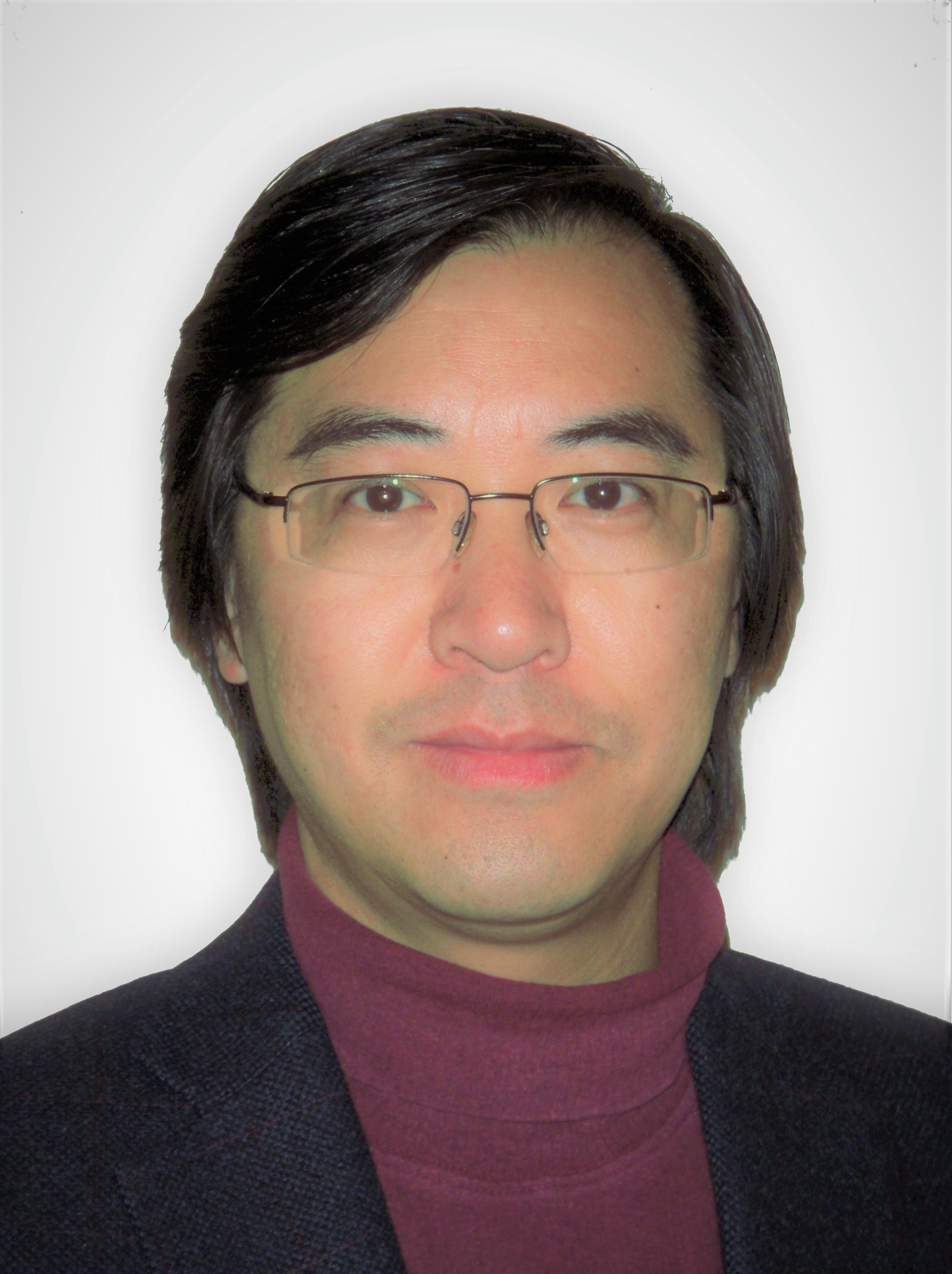 Prof Weimin M. Chen
Professor of Physics
Linköping University, Sweden
Founding director of the Swedish Interdisciplinary Magnetic Resonance Center (SIMARC)
Towards fully spin- and optically-polarized light-emitting semiconductor nanostructures for room-temperature opto-spintronics
Weimin M. Chen is a full professor in physics in the Department of Physics, Chemistry and Biology at Linköping University (Sweden) since 1999, and the founding director of the Swedish Interdisciplinary Magnetic Resonance Center (SIMARC) since 1998. He received his Ph.D. degree in materials physics from Linköping University in 1989 and completed his postdoctoral research during 1991-1993 at University of California at Berkeley (USA) before returning back to the faculty at Linköping University. His main research interests are electronic, optical, defect and spin-related properties of semiconductor materials and nanostructures, covering a wide range of materials systems including inorganic III-V and II-VI compound semiconductors, organic semiconductors and halide perovskites. His most recent research activities focus on development, understanding and exploration of novel opto-spintronic semiconductor nanostructures for future spintronic and opto-spintronic applications. He is the author of more than 700 scientific articles, 38 review articles and book chapters, and 3 books.
 Prof Andrej Kuznetsov
Department of Physics
University of Oslo
Norway
Gallium oxide polymorph heterostructures: physics, fabrication, and potential applications
Andrej Kuznetsov was awarded with his PhD degree in physics from the Russian Academy of Sciences in 1992 and accomplished his habilitation in solid state electronics in 2000 at the Royal Institute of Technology in Sweden. In 2001 he joined the Department of Physics at the University of Oslo in Norway as an associate professor and was subsequently promoted to the full professor rank in 2003. From 2018 he has acted as the Chair of the Centre of Excellence: Light and Electricity from Novel Semiconductors (LENS) - as a part of the Centre for Materials Science and Nanotechnology at the University of Oslo. His focus is to understand novel semiconductors, searching for new fundamental phenomena and enabling new device functionalities. His work resulted in more than 200 peer-review publications, scoring more then 6000 citations, h = 41 by August 2022. He taught at different levels, at present gives an introductory condensed matter physics course at the BSc level, as well as supervised numerous students at the MSc and PhD levels. He managed research funds in Sweden, Norway, as well as EU grants.
 Dr Jai Prakash
Department of Chemistry
National Institute of Technology, Hamirpur
India
Plasmonic photocatalysts: Tailoring of optical properties and advanced multifunctional applications
Dr. Jai Prakash is working as Assistant Professor in the Department of Chemistry, NIT Hamirpur. Previously, he worked as ‘INSPIRE Faculty’ in the Department of Chemical Engineering at Indian Institute of Technology (IIT) Kanpur, India (2016-2018). His PhD (2007-2012), carried out at and sponsored by IUAC (formerly, Nuclear Science Center), New Delhi, was awarded by CCS University, Meerut (India). He worked as a postdoctoral researcher at INRS-EMT, Quebec (Canada), Aix-Marseille University (France), Universite Libre de Bruselles (Belgium) and University of the Free State (South Africa). He has received several national and international scientific awards including DAAD Academic Award (2018), Merit Scholarship Award (ranked# 1) (2017) from Quebec Govt. (Canada), Promising Young Researcher Award (2016) from NRF (South Africa), Prestigious INSPIRE faculty award (2015-2016) and Young Scientist Fast Track (2012) award from DST (India), Guest scientist (2014) from NIMS (Japan), and Senior Research Fellow (2011) from CSIR (India). He has published more than 80 research articles including book/chapters in international scientific peer reviewed journals. Recently, he has been listed among World’s Top 2% Scientists List created by Stanford University (2021). His major research fields are functional nanomaterials, surface science, ion beam modifications of nanomaterials and chemistry of materials. His highly interdisciplinary research includes synthesis/characterizations of plasmonic, polymers, metal-oxides semiconductors nanomaterials, their nanocomposites for sensing, solar cell, optical, photocatalysis, SERS related environmental and energy applications.
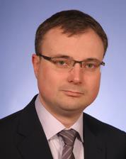 Dr Andrey Turshatov
Institute of Microstructure Technology (IMT), Karlsruhe Institute of technology (KIT)
Eggenstein-Leopoldshafen
Germany
Fundamentals and applications of upconversion in lanthanide-doped alkaline-earth fluorides
Andrey Turshatov is the Group Leader for the Materials for Spectral Conversion Group. His research interests include synthesis and photophysical characterization of luminescent materials, e.g. organic dyes, quantum dots, lanthanide-doped inorganic materials; time-resolved optical spectroscopy; photon up-conversion; light–matter interaction; super-resolution optical microscopy; functional optical materials for solar light conversion.
